The schematics for the Atari CPS Super Salt Diagnostic Assembly shows a connector labeled "Error Display Interface for Future Use". There are no schematics for this board and I haven't been able to find much information on this. Presumably this is used to display error codes, especially when the system doesn't work enough to get a display on the screen.
Besides power the signals going to the display board are the four direction pins on joystick ports 1 and 2 which can server as inputs or outputs (these are labeled D0-D7), the motor control, command and data outputs from the SIO port, and OE which is just an inversion of the command signal.
There are no schematics for this board and I haven't been able to find much information about it, but I did find a few pictures of the board. Here is a picture of the board installed in the test assembly. It is composed of two parts, the main board which plugs into the test unit with a connector at the top middle, and a second smaller display board which plugs into a card edge connector on the side of the main board.
Here is the display board. There are three empty sockets in this picture labeled CR2-CR4. CR is the reference designator for a diode so I assume these held 7-segment LED numeric displays.
You can see a device in the lower right that could be a 7-segment display, although the form factor is rather strange. There is a "C" on the PCB next to it so I assume this is CR1.
The other major component on the board is a 74LS244 octal buffer/driver with a tri-state output. This chip doesn't do any sort of latching, but it's output can be tri-stated to allow something else to control the signals the outputs are connected to.
On the main board is a oscillator circuit.
The chip is a MM5369 17 Stage Oscillator/Divider. The datasheet for this chip provides a schematic for how it is used and the appears to correspond to what we see on the board just with a fixed capacitor instead of a variable one. The amount the chip divides the clock is mask programmed at the factory so we can't determine the output frequency.
Here is one of the more interesting sections of the main board.
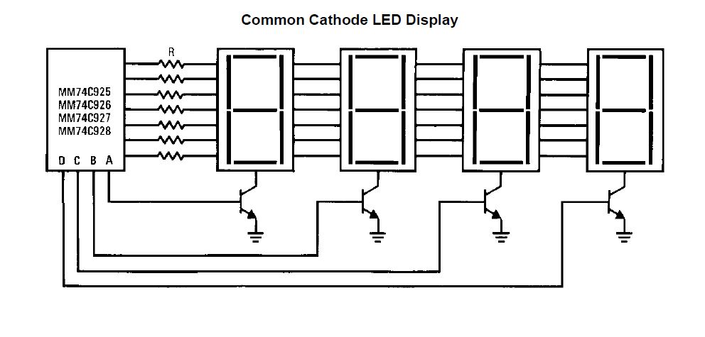
The chip in this section is an MM74C926 4-Digit Counter with Multiplexed 7-Segment Output Driver which confirms my suspicion that the display board had 7-segment LED displays on it. Once again, the schematic from the datasheet fits with the components we see on the board.
Driving a 7-segment display requires a signal for each segment, so to drive four you would normally need 28 signals. This chip simplifies this by multiplexing all four displays onto the same seven segment drivers. The cathode of the each display is sequentially activated by the chip through the transistors and this is done fast enough so it looks like all four are on at the same time. The MC74C926 has an internal counter driven by a clock so it can only display what is in it's counter. The traces from the segment drivers appear to go directly to the LED displays.
We can see on the top of the board that the 8 data signals from the first two joystick ports go directly to the display board. It's hard to see where they go from there but it looks like they may go to the 74LS244. If they do then it is possible that 74LS244 is connected to one of the LED displays so it can display either the counter output or a specific value from the computer. The output of the 74LS244 can be disabled, but I am not sure how the output from the counter would be blocked when the 74LS244 is enabled.
Here is the section of the board near the connector to the test fixture.
U1 is a MC14538B Dual Precision
Retriggerable/Resettable
Monostable Multivibrator. Basically the way this chip works is that each multivibrator has an input and and output. Activating the input, activates the output which stays active for an amount of time determined by a resistor/capacitor combination at which point it return to an inactive state. Since there are two resistor and two capacitors both multivibrators in the chip must be used. We can see that there is a trace coming off pin 15, which is controlled by one of the joystick port pins, that goes to this chip. Pin 14, another joystick pin, goes to a via which probably also connects to U1 on the back of the board. At first I though pin 15 was connected to pin 6 of the chip, which is an output, but from another angle it looks like it goes between the pins.
My best guess is that pins 14 and 15 of the interface connector go to the inputs of the two multivibrators which would allow the computer to control both the seven segment LED and to start the multivibrators.
Chip U6 contains three, three input NOR gates. Not enough of the trace are visible to determine how this chip is being used.
The remaining chips on the board are a MC14012B Dual 4-input NAND Gate, a 4040BE 12 stage ripple counter, and two 4001BE Quad 2-input NOR gates. Not enough traces are visible to know what purpose these serve.
This analysis gives some insight into how this board works, but there is still a lot of unknowns. If anyone has pictures of the back of the boards, please let me know since this would really help in figuring out how the boards works.


No comments:
Post a Comment