Monday, April 3, 2023

AMD 2901 Chip Slice

In the early days of computers, processors were build from discrete components starting with relays, vacuum tubes, transistors and then small scale integrated circuit chips. In the early 1970's the first microprocessors were introduced which made it easy to construct personal computers but they lacked the processing power needed for mini and mainframe computers. Companies like AMD provided a middle ground between these two options in the form of large scale integrated circuit chips that provided the basic building blocks of a processor. The key component of the AMD family was the 2901 chip slice.

I first encountered this chip when I was working on the MAME driver for that Atari arcade game I-Robot. I-Robot was the first arcade game to used solid filled 3d polygons. The 2901 was used as the core of a custom processor that did all the 3D calculations. 

More recently I started watching the Usagi Electric YouTube channel where he has been working on a Centurion mini-computer. You can see the playlist of videos about this project here:

https://www.youtube.com/watch?v=DJ1HwuYBuss&list=PLnw98JPyObn0wJFdbcRDP7LMz8Aw2T97V

The main CPU as well as some of the controller cards in this system were also based on the 2901.  I am going to take an in depth look at the FFC floppy controller board. You can find a lot of information about this board in this Github repository. We will start by looking at the 2901 Chip Slice Processor.

Here is the block diagram of he 2901. 


The chip has two major parts, the RAM block which is used to create 16 internal CPU registers, and the Arithmetic Logic Unit (ALU)  which does addition, subtraction and logical operations. The RAM and ALU are each 4 bits wide, but you can combine multiple chips to create as wide a data path as is needed. This is why it is referred to as a chip "slice". 

Now let's look at the inputs of the chip to better understand how it works. First there is the A and B address inputs. These are both 4 bits and select which location in memory is put on the A and B bus. To be clear there is only one block of memory, so if A and B are the same, then they are putting the same data on both busses. 

The next input is 3 bits for the source selection, this will select what goes into the two inputs of the ALU as follows:


A and B are the data selected by the A and B address inputs. Q is a temporary holding register separate from the RAM registers. D is the direct data inputs to the chip. Finally 0 makes all four bits are zero.

Next are the three function selection bits. These select the function the ALU will perform and include addition, subtraction and logical operators. 


The final control inputs, called the destination, are a little more complicated since they control destination, output and shifting. 


Lets start with the first four since they do not involve shifting. 

0 -  Transfers the output of the ALU, called F, to the Q register and also puts that output on the chip's data output, called Y. 

1- This is called no-op and just puts the ALU output on the Y output but does not store it anywhere else. 

2 - This passes the output of the ALU to the RAM location selected by the B input. The RAM location addressed by A is put on the data output. 

3 - This passes the output of the ALU to the RAM location selected by the B input and also puts on the data output.

The next four destinations do shift operations before storing the results in RAM or the Q register. Both shifts have external inputs/outputs on either end, so if a value is shifted down the low bit is available on and output and a new high bit comes in from an input. This setup allows the shift operations to work across multiple 2901s.

4 - Loads the ALU Output/2 into the B memory, Q/2 into Q and outputs the unshifted ALU output. 

5. Loads the ALU Output/2 into the B memory and outputs the unshifted ALU output. 

6. Loads the ALU Output*2 into the B memory, Q*2 into Q and outputs the unshifted ALU output. 

7. Loads the ALU Output*2 into the B memory, and outputs the unshifted ALU output.

You will notice that there is no way to get external data directly into one of the RAM registers. To do this we would use the DZ source which is external data and zero and then do a function like ADD and finally do a destination of RAMF. This will take the input, add 0 and then store it in the RAM registers pointed to by B.

Now that we have looked at the control pins, let look at the status pins. 

F=0 - This pin is used to indicate that all four outputs of the ALU are zero. This is open collector so if there are multiple 2901s, these pins will be tied together on all the chips. If any one indicates non-zero it pull the line low,. If all the chips indicate zero and external resistor pull the line high. 

OVR - This pin indicates an arithmetic two's complement operation overflowed into the sign bit. If using multiple 2901s this would only be relevant on the last (highest bits) chips. 

Cn, Cn+4 - Carry in and out

~P,~G - These are used to do a fast carry between multiple 2901s. This can be done with the Cn,Cn+4 pins but the fast carry pins allow the processor to run faster, but requires some extra hardware.

F3 - The most significant bit of the ALU output. On the last 2901 this could be used as a sign bit. 


The final two signals are for general control of the chip.

Most operations in the chip are asynchronous, but there are a couple things controlled by the CP clock input. It controls the latching of the Q registers and the RAM register outputs and also latches the data into the RAM registers. 

The final input is is Output Enable (OE) which enables the data outputs from the chip.


Wednesday, March 29, 2023

Commodore 64 Repair

Recently Josh over at RetroTV1 Tech purchased a C64 that the seller said was in working order. He wasn't able to get it working so he sent it to me to see if I could repair it. He has put up a video showing what he did to try to get the system to work. 

The system was very clean and in good condition. 


The paper shield had some sort of corrosion on it which I cleaned up before returning the system. 


The inside of the unit was also very clean. Josh had swapped the PLA chip with a modern replacement since that is a common point of failure but this did not resolve the problem. 


I unsolder the lower shield to get a look at the back of the board which looked clean and had no obvious evidence of prior repairs. 


When powering the unit up with the dead test cartridge it flashed the screen with a code the indicated a bad RAM chip. Since the RAM chips were soldered in I wanted to rule out everything else before replacing the RAM chip. So I started by swapping the PLA and the SID with a known good unit. I also tried swapping in the original PLA. I was getting very strange results during this process. It took a while but I eventually figured out what I was doing wrong.

Here is a picture of Josh's C64 with the locations of the PLA and SID.


Mine had a slightly different PCB rev and you can see here that the positions of the PLA and SID were revered. The chips have the same number of pins so I was mistakenly putting them in the wrong sockets!


With that worked out I was quickly able to determine the Josh's C64 had a bad SID and that his original and replacement PLAs were fine. Whatever was wrong with the SID was appearing as a RAM failure. I happened to have a spare SID in my chip collection, no idea where I got that from because I never did any C64 repairs, so I put that one in and that got the dead test working. Even though this SID allowed the system to work, I was getting really bad sound out of it so we ended up getting a modern replacement SID. We chose the ARMSID which has a really nice sound to it.

Next step was to remove the dead test cartridge and boot the system normally. When I did this I got just a black screen. I did some research and the most common cause is a bad Kernel ROM. I swapped that with the one in my system and confirmed it was the cause. 

The C64 ROMs have a different pinout then standard EPROMs. Since I have an EPROM programmer and the parts on hand I decided to try to build an EPROM adapter as shown on this page:


Here are a few pictures of that build process. You can also buy a PCB for this that makes the process a lot easier. 


This adaptor worked ok, but Josh decided to get a modern replacement since it would be more reliable.

With all these problems worked out, the final step was to replace the electrolytic capacitors in the system. This is a great site for cap kits, the provide the kits and good instructions on how to replace them. When you buy a kit be sure to get the one that matches the version of the PCB your system has.


The system has quite a few electrolytic caps that need to be replaced. Be sure to read the instruction on the web site since the replacements are not all identical to the originals. 


Josh will eventually be doing a video to show of the repaired system.


Sunday, March 26, 2023

CPS Super Salt - Error Display Board

The schematics for the Atari CPS Super Salt Diagnostic Assembly shows a connector labeled "Error Display Interface for Future Use". There are no schematics for this board and I haven't been able to find much information on this. Presumably this is used to display error codes, especially when the system doesn't work enough to get a display on the screen.

Besides power the signals going to the display board are the four direction pins on joystick ports 1 and 2 which can server as inputs or outputs (these are labeled D0-D7), the motor control, command and data outputs from the SIO port, and OE which is just an inversion of the command signal. 

There are no schematics for this board and I haven't been able to find much information about it, but I did find a few pictures of the board. Here is a picture of the board installed in the test assembly. It is composed of two parts, the main board which plugs into the test unit with a connector at the top middle, and a second smaller display board which plugs into a card edge connector on the side of the main board. 


Here is the display board. There are three empty sockets in this picture labeled CR2-CR4. CR is the reference designator for a diode so I assume these held 7-segment LED numeric displays.


You can see a device in the lower right that could be a 7-segment display, although the form factor is rather strange. There is a "C" on the PCB next to it so I assume this is CR1.


The other major component on the board is a 74LS244 octal buffer/driver with a tri-state output. This chip doesn't do any sort of latching, but it's output can be tri-stated to allow something else to control the signals the outputs are connected to. 

On the main board is a oscillator circuit. 


The chip is a MM5369 17 Stage Oscillator/Divider. The datasheet for this chip provides a schematic for how it is used and the appears to correspond to what we see on the board just with a fixed capacitor instead of a variable one. The amount the chip divides the clock is mask programmed at the factory so we can't determine the output frequency. 

Here is one of the more interesting sections of the main board. 


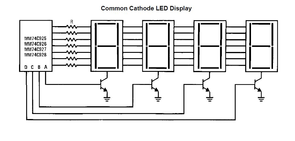
The chip in this section is an MM74C926 4-Digit Counter with Multiplexed 7-Segment Output Driver which confirms my suspicion that the display board had 7-segment LED displays on it. Once again, the schematic from the datasheet fits with the components we see on the board. 

Driving a 7-segment display requires a signal for each segment, so to drive four you would normally need 28 signals. This chip simplifies this by multiplexing all four displays onto the same seven segment drivers. The cathode of the each display is sequentially activated by the chip through the transistors and this is done fast enough so it looks like all four are on at the same time. The MC74C926 has an internal counter driven by a clock so it can only display what is in it's counter. The traces from the segment drivers appear to go directly to the LED displays. 

We can see on the top of the board that the 8 data signals from the first two joystick ports go directly to the display board. It's hard to see where they go from there but it looks like they may go to the 74LS244. If they do then it is possible that 74LS244 is connected to one of the LED displays so it can display either the counter output or a specific value from the computer. The output of the 74LS244 can be disabled, but I am not sure how the output from the counter would be blocked when the 74LS244 is enabled.

Here is the section of the board near the connector to the test fixture.


U1 is a MC14538B Dual Precision Retriggerable/Resettable Monostable Multivibrator. Basically the way this chip works is that each multivibrator has an input and and output. Activating the input, activates the output which stays active for an amount of time determined by a resistor/capacitor combination at which point it return to an inactive state. Since there are two resistor and two capacitors both multivibrators in the chip must be used. We can see that there is a trace coming off pin 15, which is controlled by one of the joystick port pins, that goes to this chip. Pin 14, another joystick pin, goes to a via which probably also connects to U1 on the back of the board. At first I though pin 15 was connected to pin 6 of the chip, which is an output, but from another angle it looks like it goes between the pins. 
 

My best guess is that pins 14 and 15 of the interface connector go to the inputs of the two multivibrators which would allow the computer to control both the seven segment LED and to start the multivibrators. 

Chip U6 contains three, three input NOR gates. Not enough of the trace are visible to determine how this chip is being used. 

The remaining chips on the board are a MC14012B Dual 4-input NAND Gate, a 4040BE  12 stage ripple counter, and two 4001BE Quad 2-input NOR gates. Not enough traces are visible to know what purpose these serve.

This analysis gives some insight into how this board works, but there is still a lot of unknowns. If anyone has pictures of the back of the boards, please let me know since this would really help in figuring out how the boards works.


Saturday, March 25, 2023

Atari CPS Super SALT - Joystick Ports

The final part of the CPS Super SALT test fixture we will look at is the joystick ports.

The four directional pins on the joystick ports can be can be configured as either inputs or outputs, so an output on one can be read as an input on another. The direction pins on port 1 are connected to port 3, and the pins on port 2 are connected to port 4, this allows for the testing of all the direction pins. If the test is being run on an XL series computer the analog switch U12 is enabled which connects the direction pins on port 1 to port 2. 

The trigger inputs are connected to the direction pins as follows:

Trigger J1  -J1(3)
Trigger J2 - J2(3)
Trigger J3 - J3(1)
Trigger J4 - J4(1)

The paddle inputs are connect through resistors to direction pins as follows:

Pot J1(A) - J1(4)    
Pot J1(B) - J1(3)
Pot J2(A) - J2(4)
Pot J2(B) - J2(3)

Pot J3(A) - J3(2)    
Pot J3(B) - J3(1)
Pot J4(A) - J4(2)
Pot J4(B) - J2(1)


Friday, March 24, 2023

Atari CPS Super Salt - SIO Test

This is the next in a series of posts about the Atari CPS Super Salt Test Assembly. In this post I will look at the SIO test. 

Lets start by looking what is basically the middle of the circuit. U1 is a 4053 analog switch IC, redrawn here to make it easier to understand. This chip is basically three switches each of which is controlled by a digital input. 

Switch A is used for the clock input to the computer. It is controlled by pin 1 of the first joystick port and can switch between a baud rate generator and the output clock from the computer. Looping the out clock to the in will test these pins on the port, but this would not validate that the computer is sending data at the correct clock speed, thus the need for the baud rate generator. 

Switch B is used for the data to the computer. It is controlled by pin 2 of the first joystick port and can be switched between a data generator and the data output from the computer. 

Switch C is used for the SIO audio input. It is controlled by pin 3 of the first joystick port when the Motor Control output of the SIO port is high. It can either be unconnected so there is no audio input, or it can be connected to switch A so it can get either the output clock or the baud generator. There is no way for the computer to actually sample the audio input so this test relies on the operator listening for tones. 

Now lets look at the SIO connector. Pins 1,2,3 and 5 are the clock and data inputs and outputs. As we saw above these connect to the analog switch which allows these to be tested in various ways. Pin 7 is the command output which connects to Interrupt input thus allowing those two signals to be tested. Likewise, the Motor Control output is connected to the Proceed input. Pin 10 is just a +5v output from the computer so goes to the ADC as described in my previous post. Pin 11 is the audio input which was described above. Finally, pin 12 is a +12V output on the 400/800 and also goes to the ADC.

There appears to be a mistake in this section of the schematics. The output of inverter U11 is used to control certain test modes through U2. You can see that the input to the pair of inverters is connected through a resistor to ground which would leave no way for this signal to be controlled. There is a wire coming from Motor Control that crosses between the resistor and Pin 11 of U11, so I believe there is supposed to be a connection there so Motor Control becomes the input to those two inverters. 


Next lets look at the baud rate generator, U6. The clock starts from 1.8432 MHz crystal oscillator which is then divided down into 6 baud rates, 9600, 4800, 2400, 1200, 600 and 300. If pin 4 of joystick port 1 or 2 is set low, this will bring RSA high and provide a 19200 baud rate, and a 76.8 KHz clock to the ADC. The clocks go to data selector U5 and one is selected based on the value on pins 1-3 of  joystick port 1 or 2 and is passed to U1 as described above. 


The final section of the SIO test is the data generator. This section starts with a binary counter clocked from the baud rate generator. The counter counts from 0 to 15 and drives a 16 bit data selector U3. The inputs of the data selector are setup to generate a serial sequence of 0000101010101000 which can be fed to the SIO input of the system being tested.,  


Sunday, February 19, 2023

Atari CPS SuperSALT Test Assembly ADC

In my last post I introduced the Atari CPS SuperSALT Test Assembly which is used as part of the SuperSALT test to verify the ports on the Atari computer. The test assembly has a number of test functions, so the first one I will look at is the Analog to Digital Convertor (ADC). 


The ADC is part number ADC0816. It has 16 channels and 8 bit resolution. You can see a data sheet here. The channels are assigned as follows:

0 – Onboard 5 volt
1 – 5 volt from SIO port
2 – 5 volt from J1 Port
3 – 5 volt from J2 Port
4 – 5 volt from J3 Port (400/800 only)
5 – 5 volt from J4 port (400/800 only)
6 – Ground from Serial Port
7 – Ground from J1 port
8 – Ground from J2 port
9 – Ground from J3 port (400/800 only)
10 – Ground from J4 port (400/800 only)
11 – Motor control line from SIO port
12 – 12 Volt line from SIO port (400/800 only)
13 – Positive half-cycle current draw (400/800/1200XL)
14 – Negative half-cycle current draw (400/800/1200XL)
15 – Onboard ground line

Which channels are tested is based on the type of machine. The XL series computers only have two joystick ports so the channels for the other two are not needed for these computers. The 400 and 800 supply 12 VDC on pin 12 of the SIO connector, but this is absent on the XLs. The current measurements are done by passing the power from the AC adaptor through the test box so the current draw can be measured. This only done on the 400 and 800 since the current measurement circuit is designed to measure the 9 VAC input voltage they use. 

The ADC is controlled with a combination of joystick ports 1 and 2 and the data signal from the SIO port. The sequence for reading the ADC is as follows:

1. Set PORTA (which controls joystick ports 1 and 2) to output
2. Write the ADC channel number to bits 0 - 3 of PORTA and set bit 7 to 0 to switch the baud rate generator to fast clock.
3. Wait approximately 1280 CPU cycles.
4. Set bit seven of SKCTL to 1 to latch the channel number and reset the ADC.
5. Wait approximately 1280 CPU cycles.
6. Set bit seven of SKTCL to 0 to start the ADC.
7. Wait approximately 2560 CPU cycles.
8. Set PORTA to input. 
9. Read the eight bit ADC value from port A.


Atari CPS SuperSALT Test Assembly


The CPS SuperSALT was a system used to test Atari 8-bit computers (400/800/XL) both in a factory setting and for after market repair. The system was composed of a cartridge with the test software and a special test assembly that was build into Atari 850 interface module case. The assembly is needed to completely test the Joystick and SIO ports. 

Here are pictures of two different version of the test assembly.

REV O:


REV C:

The technical reference manual for this device can be found here:

http://www.atarimania.com/documents/CPS_Supersalt_Technical_Users_Manual.pdf

That manual contains schematics that appear to be for the Rev O board since it has a power switch which is absent on Rev C.

There is also an Error Display add on board. In the schematics this is labeled "for future use", but I do have pictures of board, although there are no schematics available for it. 

Over my next few posts I will talk about how this device worked.